Revolutionizing Wafer Test Processes: The AOP PCI Metrology and Inspection Solution
Revolutionizing Wafer Test Processes: The AOP PCI Metrology and Inspection Solution
Wafer test is one critical step in the manufacturing of semiconductors as it comes along with certain risks for losses from a productivity point of view, and is also known to be the source of expensive quality issues with even more severe implications.
The Challenges of Final Wafer Testing
When a wafer undergoes a final test of its functional structures, the complete chain of value creation in the front-end-of-line (FEOL) processes is completed. Sometimes, even back-end-of-line (BEOL) process steps, such as bumping, are applied to the wafers already. This, in turn, means that a loss of a number of components, or even complete wafers caused by final wafer test, poses a strong negative impact to the capitalization of products at a very late stage.
Further complicating the situation is the fact that many semiconductor manufacturers do not move tested wafers to their own internal or outsourced BEOL processes, but also deliver the tested wafers to their customers directly. This means that there is another effect that may even be more critical than the productivity losses mentioned: It could happen that, during the final wafer test, wafers can become damaged completely unnoticed; there are a number of well-known examples of such damage having caused costly product recalls in the past.
Addressing Probe Card Damage
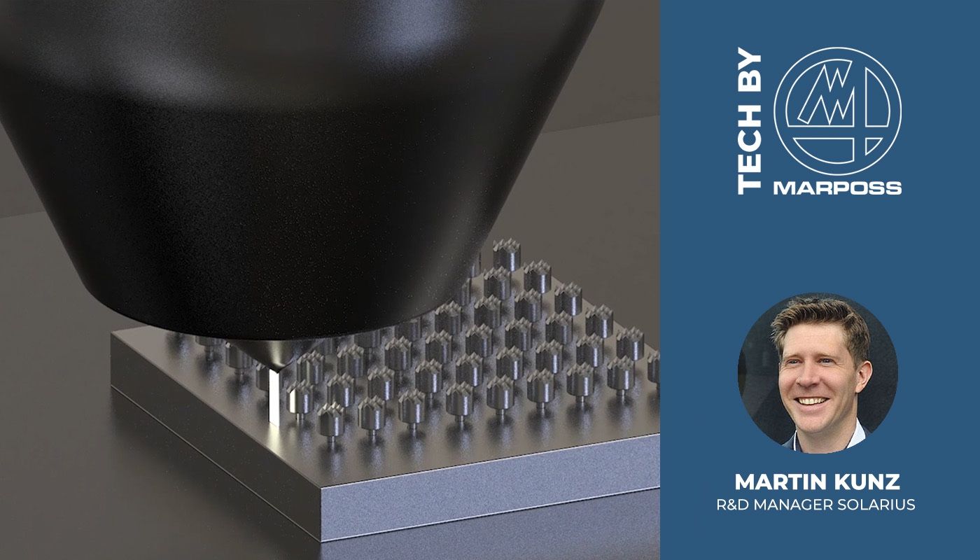
While there are a number of pain points that cause damage that can go unnoticed during final test, it is the damaging of wafers by defect probe cards that is the focus of the AOP PCI metrology and inspection tool Defect probe cards can cause significant productivity losses during final wafer test or, in the case of damage that goes unnoticed, product recalls with unpredictable consequences. In comparison to probe card related damage that is detected before shipment to end users and that certainly causes financial loss, damage that goes unnoticed will result in wafers being shipped to customers. These damaged wafers will eventually be discovered—but only after they have already compromised production lots.
The worst case will be when the defective components become part of more expensive packages comprising multiple functional elements. If the damage continues to be undetected until the final test of the end packaged “system,” the financial losses are even greater, not to mention the losses that occur if these devices are shipped to end users such as automotive manufacturers. While this scenario can seem overly dramatic, it has happened before—and all because of an undetected defect probe card.
With the above mentioned in mind, along with its financial consequences and implications for a company’s business reputation, how could such events be avoided?
Fast probe card inspection process
One way is to apply a fast probe card inspection process that enables a clear decision to be made about whether a probe card is “OK” for testing or not. Such an idea, however, is far from being applicable to the reality of a wafer test operation.
Therefore, a closer look at the implied requirements must be taken. To the point, the following requirements are needed to ensure an intact wafer after test:
- A continuous and reliable observation of a probe card to identify unwanted objects. This will allow one to make a decision about whether there will be any imprinting of a wafer or not.
- A continuous and reliable observation of the geometric parameters of the probe tips. This will allow one to make a decision about whether the probe tips are going to “scratch” or “scrub” the contact pads on a wafer correctly or not.
- The observation of aforementioned conditions and parameters must be fast, which will allow one to check and re-check probe cards often, thereby enabling a closed-loop observance of probe card conditions during the process.
Besides the information about possible damage to a wafer emerging out of probe card conditioning, one could also derive process control relevant information from such a probe card inspection process.
The precise assessment of probe tip geometries allows one to judge in advance about whether a tip will assure proper mechanical pre-conditions for a good electrical contact to the pad.
The precise assessment of probe head geometry allows conclusions about temperature-related changes of a probe head surface that can lead to different “scrubbing” or “scratching” behavior.
The fast feedback allows one to check and re-check probe cards frequently following touchdown counters or production lots processed.
The continuous availability of information about probe tip and probehead conditions can be correlated with scrubs by statistics when doing automated optical inspection (AOI) after the testing. This is especially interesting in terms of the probe head, as “scrubbing” or “scratching” behavior essentially depends on the probe head shape and positioning.
The fast feedback and the detailed failure information of the process allows shorter and more focused repair and maintenance cycles. The nature of a defect and its location can be pointed out fast and clearly, and a full re-assessment of a probe card can be done very quickly before the probe card is routed back to the process.
The AOP PCI Metrology and Inspection System
Having well understood the necessity of a process capable of the aforementioned requirements, Solarius developed, together with a customer, a tailor-made solution for wafer test sites to address the typical pain points leading to productivity losses and quality issues. The result of that collaboration is the AOP PCI inspection and metrology system. This tool enables a process that allows one to frequently assess a probe card’s overall condition in the wafer testing process following the requirements described above, being fitted to all major tester interfaces. The AOP PCI tool is designed according to SEMI standards and incorporates a SECS/GEM interface.
The tool also works in conformance with established probe card analyzing tools and therefore does not introduce new or deviating information to existing processes. The AOP PCI can be equipped with a re-work station to allow direct repair inside the tool and can be offered in an upside-version to support OHT loading of probe cards.